The manufacturing of a PCB involves several stages that require precision and quality control to ensure the final PCB meets the desired specifications and performance standards.
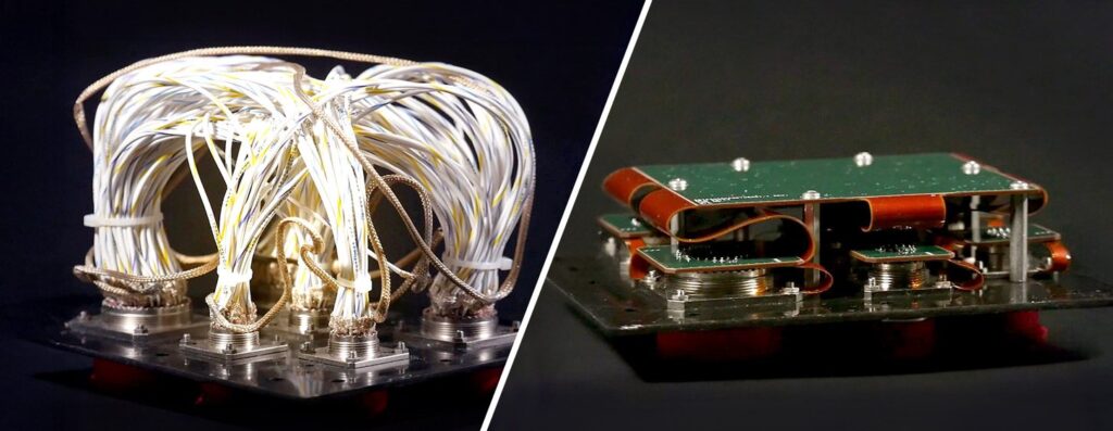
At Pioneer Circuits, we often say that every flex and rigid-flex circuit we build carries both innovation and responsibility. The manufacturing process behind these boards is a precise blend of materials science, engineering discipline, and decades of hands-on expertise. Each step is designed to translate a customer’s schematic into hardware capable of surviving the harshest environments, whether it’s orbiting Earth, landing on Mars, or defending the skies.
PCB Manufacturing Process Step by Step
Step 1: Printing the design/copper

The laminate plate is covered with resist, a photo-sensitive film that hardens after exposure to ultraviolet (UV) light. Targeted UV light exposure hardens the resist where the copper pathways need to be preserved, while copper areas meant to be removed remain unhardened.
step 2: chemical etching process

The board is then washed with an alkaline solution to remove the unhardened resist, leaving only the intended hardened (cured) resist to protect the desired copper areas. Then, a chemical etching process removes the exposed, unprotected copper, forming the circuit patterns as designed.
Step 3: lamination

The layers of copper foil, dielectric, and prepreg are then laminated together via a press that applies heat and pressure or by autoclave. An autoclave laminates layers by applying uniform heat, vacuum, and high pressure within a sealed chamber, causing the prepreg resin to flow, fill voids, and cure into a rigid, void-free bond across the entire stack.
step 4: Drilling
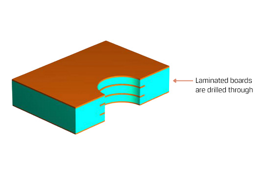
The next step involves drilling holes for component leads and vias and to form connections between individual layers.
step 5: plating
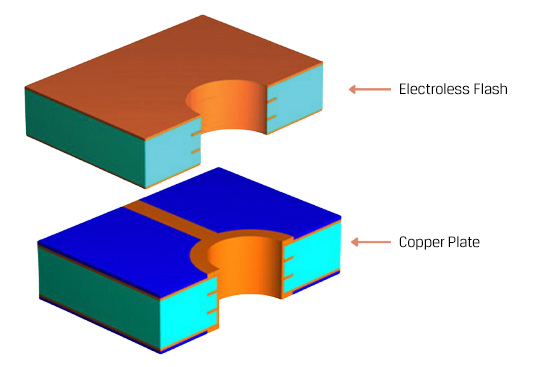
The plating process involves depositing a thin layer of copper, either through electroless plating (a chemical process that coats the drilled holes and panel surfaces without electricity) or electroplating (which builds up the copper thickness using an electrical current). This conductive copper layer, typically only a few thousandths of an inch thick. Covers the outer surfaces and the walls of drilled holes, creating the electrical pathways that connect the PCB’s layers.
step 6: Solder mask application
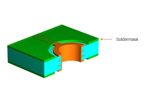
A liquid or dry film solder mask is then applied and cured. When exposed to UV light, the solder mask hardens over the copper traces that need protection, while the unexposed areas remain soft and are developed away. This process both shields the copper from damage and oxidation and defines the openings where solder will later be applied.
step 7: legend printing
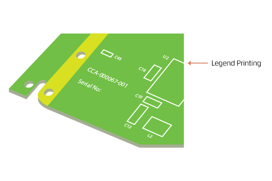
Legend is the process of adding markings per customer request to the surface of the board with ink. This information can include the cage code numbers, warning labels, part numbers, and more to help assist with future processing such as assembly and traceability.
step 8: Surface finish
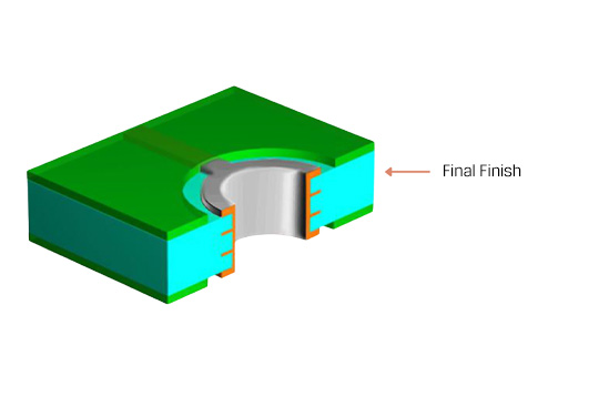
After printing the information onto the boards, a final finish (e.g., Hot Air Solder Level, fuse, ENEPIG) is applied. This finish is a protective coating, covering exposed copper areas to prevent oxidation and improve solderability.
The Pioneer Circuits Advantage
With over 40 years of experience, Pioneer Circuits offers reliable and high-quality rigid, flex, and rigid-flex PCBs that meet the demands of critical industries requiring consistent functionality.
Learn more about our Manufacturing capabilities below.